Controllable doping in a perovskite semiconductor enables ultra-bright LEDs
Semiconductors are at the heart of the modern electronic industry. The ability of controlling the polarity and concentration of electric charges in semiconductors have led to revolutionary inventions including diodes, transistors, solar cells, detectors, LEDs and semiconductor lasers. For typical semiconductors, the control of the electrical properties is achieved by “doping”, the inclusion of impurity elements into the crystal lattices. For instance, the introduction of boron into silicon turns it into a positive (p-) type semiconductor mainly conducting positive charges, while the inclusion of phosphorous turns silicon into a negative (n-) type semiconductor mainly conducting negative charges.
Metal halide perovskites are a new class of semiconductor exhibiting great performance in optoelectronic applications such as solar cells, LEDs and lasers, and are easily producible at low cost. Despite the rapid progress in this emerging field, the mechanisms of reliably controlling doping in perovskite semiconductors are yet to be found.
Recently, researchers at Zhejiang University discovered that the polarity and charge concentration of an emissive perovskite semiconductor can be controlled by the incorporation of a molecular dopant. A continuous transformation from n-type to p-type behaviors in the perovskite material was achieved, while retaining very strong emissive properties. The controllable doping leads to the demonstration of high-efficiency (28.4%) perovskite LEDs with a simple device structure, achieving record-breaking brightness (over 1.1 million cd/m2) amongst all classes of solution-processable LEDs (including OLEDs, quantum dot LEDs and perovskite LEDs). The related research paper entitled “Controllable p- and n-type behaviours in emissive perovskite semiconductors” was recently published in Nature (Xiong et al, Nature (2024), https://doi.org/10.1038/s41586-024-07792-4). The corresponding authors of the paper are Prof. DI Dawei and Prof. ZHAO Baodan of Zhejiang University. XIONG Wentao is the first author of the paper.
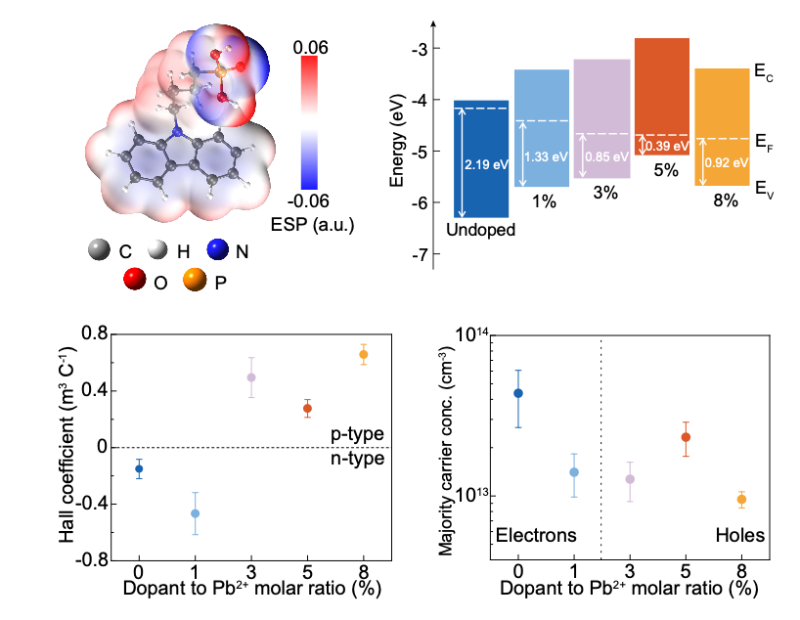
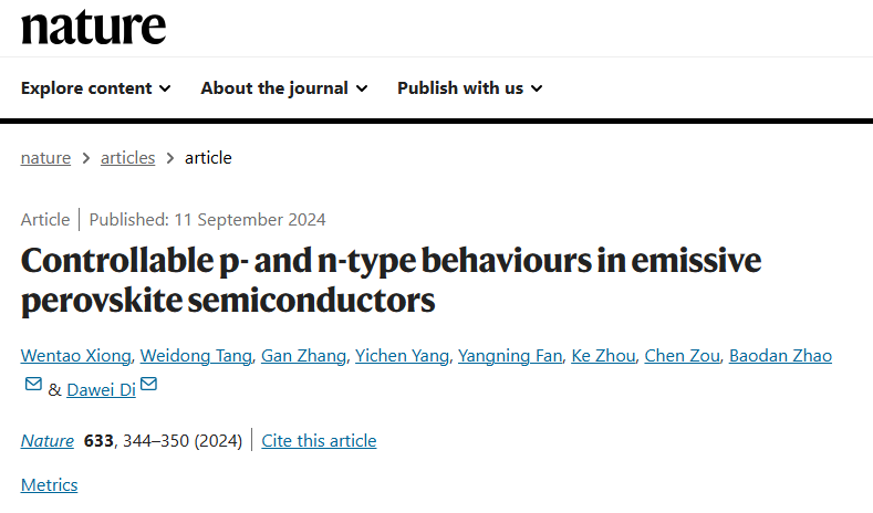
Figure 1: p-type to n-type transition in a perovskite semiconductor. Source: Nature (2024).
“Perovskites are a class of semiconductor, so they are expected to show semiconductor properties”, said Prof. DI Dawei, Deputy Director of the International Research Center for Advanced Photonics of Zhejiang University. “A range of experiments conducted by us show that the Fermi level, the expected energy of the electrons, moves gradually from the higher-energy side to the lower-energy side across the bandgap of the perovskite semiconductor. This means that the semiconductor transforms from n-type which is in favor of conducting electrons (negative charges), to p-type which is in favor of conducting holes (positive charges). The charge carrier polarity and concentrations can be adjusted by the doping process, as the Hall effect measurements tell us”, said DI
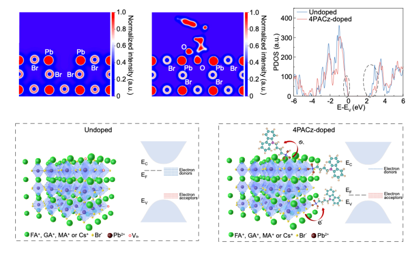
Figure 2: The molecular doping process. Source: Nature (2024).
“The dopant used for controlling the electrical properties was a molecular material called 4PACz, which was used in earlier studies to form an ultrathin molecular layer in efficient perovskite solar cells”, said Prof. ZHAO Baodan of Zhejiang University. “In our study, these molecules were found to work as an effective dopant for the perovskite semiconductors. Quantum chemical calculations reveal that the molecules show strong electron withdrawing abilities, effectively acting as a p-type dopant for the perovskite. Similarly, n-type dopants for perovskites were also found by us.” said Zhao.
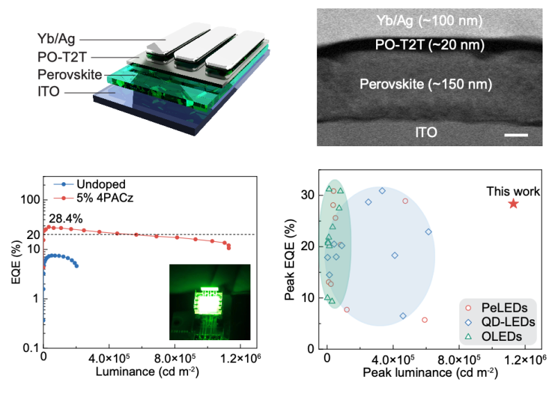
Figure 3: Performance of hole-transport layer-free PeLEDs. Source: Nature (2024).
XIONG Wentao, the first author of the paper, is a PhD student supervised by Profs. DI and ZHAO. He said: “Using this type of doped perovskite materials, we can build devices with new structures and better performance. For example, with a p-type perovskite, we could fabricate perovskite LEDs without any hole-transport layers.” “The perovskite LEDs we made achieved very high external quantum efficiencies of up to 28.4%. The energy-conversion efficiency of the devices reached 23.1% - the highest for visible perovskite LEDs”, said Xiong. “Surprisingly, these perovskite LEDs were extremely bright. The highest brightness achieved was 1.16 million cd/m2 (1.16 million nits) – this is a new record for the brightness of solution-processable LEDs, including OLEDs, quantum-dot LEDs, and perovskite LEDs”,said Xiong.
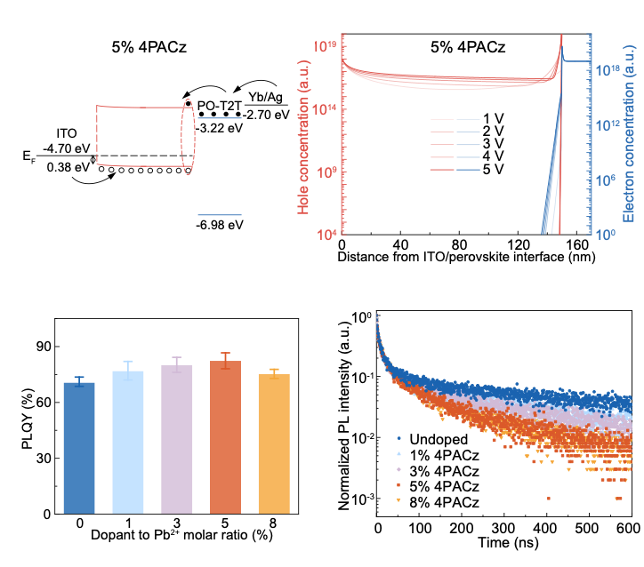
Figure 4: Mechanisms of device performance improvements. Source: Nature (2024).
The underlying reasons for the exceptional device performance were investigated by device modelling and optical measurements, which align very well with the device working mechanisms hypothesized by the researchers. The ability of controlling the polarity and concentration of charge carriers in perovskite semiconductors indicates the possibilities in creating new device designs and functionalities. The researchers created initial demonstrations of p-n junction diodes based on perovskite semiconductors. The controllable doping of perovskite semiconductors is expected to lead to a new generation of optoelectronic devices.
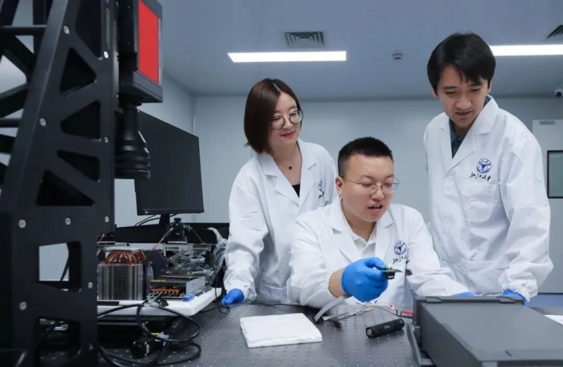
Researchers testing perovskite devices in the lab. [from right to left] Prof DI Dawei, XIONG Wentao, and Prof. ZHAO Baodan.
In November 2020, a team of researchers lead by Professor DI Dawei joined the International Research Center for Advanced Photonics, International Campus, Zhejiang University. From then on, International Campus puts great emphasis on maintaining a growth-oriented environment for its talent and makes sure the research team is equipped with sufficient laboratory and office space. The city of Haining has provided special funding for thetransm.
Having established a world-class platform for advanced fabrication and characterization at the international campus, the team is currently conducting fundamental and cutting-edge research on novel semiconductor optoelectronic devices, which includes multiple laboratories focused on advanced characterization, micro-nano fabrication, ultrafast spectroscopy, luminescent devices, energy optoelectronics, electronic devices, materials chemistry, and flexible optoelectronics. To date, nearly 20 graduate students and 10 postdoctoral researchers are stationed in the laboratories on campus.
"I was the first doctoral student in Professor DI’s group who’s based in the International Campus," recalls XIONG Wentao, the first author of the paper and a PhD student (2020 intake) at Zhejiang University. He reflected on his time visiting the campus, “we were greatly impressed by its international environment and spacious laboratories. We all felt that this was a great place for research." XIONG added, "the excellent laboratory facilities and platforms, the international and interdisciplinary research atmosphere, as well as the comprehensive support provided by the campus, along with the kind guidance and help from professors DI and ZHAO, enable us to focus on truly important research topics and foster our creativity and active thinking. These factors are indispensable for us in achieving significant research results."
Professor DI Dawei’s research team focuses primarily on novel semiconductor optoelectronic devices and device physics, exploring new luminescent mechanisms in organic and perovskite semiconductors, and has set a number of performance records. They achieved controllable electrical doping in perovskite semiconductors and established a brightness record for perovskite LEDs, realized ultralong-lifetime perovskite LEDs, and revealed the unified physical mechanism of ultra-low voltage LEDs. Over the past five years, they have published several influential papers in journals such as Nature, Nature Photonics, Nature Nanotechnology, Nature Electronics, Nature Communications, and Science Advances, garnering widespread attention from the international research community.
Related paper:
Xiong, W. et al, Controllable p- and n-type behaviours in emissive perovskite semiconductors. Nature (2024). https://www.nature.com/articles/s41586-024-07792-4
Sources: Prof. DI Dawei, Prof. ZHAO Baodan, XIONG Wentao and co-authors; Nature (2024).
Source: Global ZJU
Article: MA Yudan, ZHA Meng, YANG Dehang
Photography: LU Shaoqing, LIANG Xiaohan, DI Dawei’s research team
Editing: ZHANG Shufan, ZHOU Yiying, LI Yinan, LIU Shuaiyin
Edinting in charge: ZHOU Yiying, ZHANG Yi
Reviewer: YANG Yi
Translation: DI Dawei’s research team, LIU Shuaiyin